

For years, the answer to “what is the best cold plate you can buy” has been the same. Pure copper skived fins, around 100 µm thick at around 100 µm pitch, shaved from a solid block in one operation. Cheap, repeatable at tens of millions of units, and very, very good.
Skived fin designs have set the bar for a reason that is based in physics, not marketing: Q = h · A · (T₂ − T₁).
Heat transfer scales with area, and area scales with the square of the feature size. Halve a fin and you don’t get a slightly better plate, you get a considerably better one. Skiving is very good at making very small features very cheaply, so every alternative that tried to win by adding surface area lost, and usually lost expensively.
We spent a fair amount of time trying to win that fight before accepting we couldn’t. So we stopped competing on surface area and fundamentally re-thought the problem. This is that story.

The benchmark
Before we start, take a look at the graphic below, which presents the skived-fin benchmark. Every number in this post is measured against this.

ToffeeX against three skived baselines
We ran a customer cold plate through our generative design process and benchmarked it against skived-fin plates at 100, 80, and 50 µm. Same heat load, same footprint, same coolant, high-fidelity conjugate heat transfer on all of them.

Against the 100 micron plate, we came out 6.7% better on thermal resistance and paid about 36% more pressure drop for it. That’s a trade, for sure and we have no intention of hiding this, because ultimately the real wins came as we tried to push the skived fin designs further by reducing the fin thickness and pitch further — down to 80 microns.
But, it turns out that against an 80 micron plate, ToffeeX came out strictly better. The design was Pareto-dominant over the 80 micron skived fin design. Better heat transfer and around 10% lower pressure drop.
And if we went even further, against a 50 micron skived fin design, ToffeeX delivered comparable cooling for roughly a third of the pumping power.

Why it works: conduction versus convection
A skived fin array is a conduction machine. Thin, dense, highly conductive copper carries heat off the baseplate and presents it to the coolant over an enormous wetted area. The coolant’s job is mostly to be there. The only way you have to improve it is to make the fins thinner and denser, and every time you do this, you pay significantly in an increased pressure drop, because you are forcing the same flow through narrower channels.
Our plates work the other way round. The optimiser solves the fluid and the thermal fields together, so the geometry it produces is shaped by what the flow is doing rather than by what a designer thought the flow might do. You end up with recirculation, controlled separation and reattachment, structures that keep tearing up the thermal boundary layer instead of waiting for metal to carry heat away.

That is a different mechanism, and it has a different scaling behaviour. It does not need a 100 µm fin to work, because the length scale that matters is the scale of the flow structures doing the cooling, not the thickness of a solid feature. That scale is what our optimisation resolves, and it is comfortably inside what additive manufacturing can build.
Which is the real headline here. We are not matching skiving on its own terms. We beat a finer-featured plate without needing to match its feature size at all.
ToffeeX designs cut pressure drop so sharply that we can push more coolant through the plate for the same pumping budget. At 1.0 m/s, the compressed ToffeeX design reaches the same 61 °C peak as the 100 µm skived fins at 0.3 m/s, with a third of the pressure drop. Lower losses buy higher flow, and higher flow buys lower temperatures.

Yes, you need Additive Manufacturing for this
A geometry like this cannot be machined, cast or skived. It exists because metal additive manufacturing exists. But printing it at all is not the only difficult part.
The hard part is that AM starts at a disadvantage on every axis that a cold plate cares about.

Copper LPBF holds a minimum wall thickness of around 300 µm against skiving’s 100 µm. As-built conductivity sits near 76% IACS because of residual porosity, recovering toward 96% only after heat treatment (if you’re lucky). As-built roughness runs Ra 3 to 19 µm, while the pedestal needs something like 0.001 in/in flatness to keep TIM contact resistance under control (so post-processing is not optional). And the volumes are unforgiving: tens of millions of plates per chip generation, each one needing repeatability, leak integrity, and inspection.
This is why we don’t check manufacturability at the end. Printable wall thickness and self-supporting features for the orientation need to be built in from the beginning, as constraints on the topology optimisation process from the start.
What comes out of ToffeeX is production geometry, not a concept a manufacturing engineer then has to redraw. It goes to an AM partner and gets built (watch this space for further).
… And does the money work?
Not as an energy story, no.
Once you’re on direct-to-chip liquid, there isn’t much cooling headroom left to reclaim, so from an energy savings perspective we don’t really think it makes sense.
The money is in throughput for the next generations of ultra-high power chips. Lower junction temperatures mean less thermal throttling, which means more sustained compute out of the megawatts you already have.
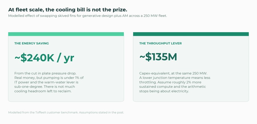
At a 250 MW fleet, the pressure drop reduction is worth roughly $240K a year in pumping energy. Assume around 2% more sustained compute from the lower junction temperature and the capex-equivalent value lands near $135M. At that point, the unit cost of the plate stops being the interesting number.


